最佳晶片驗証工具
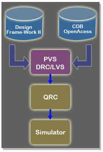
Cadence® Physical Verification System(PVS) 是由 EDA 軟體商 Cadence 所提出之新一代晶片驗証工具,它不僅能使用於類比/數位/混合訊號之設計平台,如 Virtuoso IC Layout Platform、Encounter,且更與寄生參數萃取軟體整合,如 QRC,以萃取佈局後寄生參數,提供使用者在晶片後段驗証的完整解決方案。
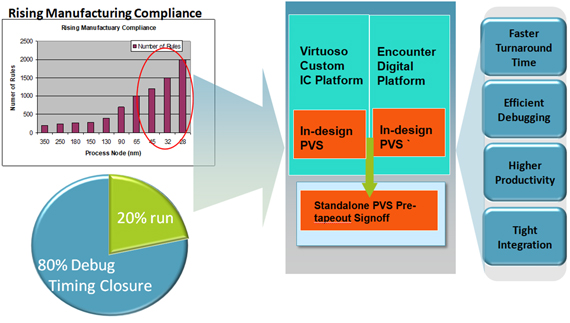
隨著半導體製程微縮的發展趨勢,晶片後段驗証 (Back-end Verification) 所耗費的處理時間與複雜度不斷提昇的情況下,Cadence® Physical Verification System (PVS) 驗証工具,憑其線性化的優異性能表現 (Performance),不僅能減少運算處理時的等待時間;另外其創新的即時偵錯 (Time-To-Error) 功能,即時偵錯已運算完成部份,讓使用者不再浪費時間等待運算結果,再者,其新創的人性化圖形除錯界面 (Graphic LVS Debug Interface ) 及互動式短路偵察系統 (Interactive Short Locator),不僅能有效彌補偵錯經驗不足的困擾,更能有效縮短來回除錯所耗費的時間 (Turn Around Time),以提昇工程師的效率及晶片產出。
此外,Cadence® Physical Verification System (PVS) 不僅同時支援 GDSII 與 Open-Access 的格式,亦相容於目前工業界標準的驗証語言,以降低工程師跨平台使用上的額外工作與難度。
Physical Verification System (PVS) 流程圖
Physical Verification System (PVS) 後段驗証解決方案
Physical Verification System (PVS) 特點
PVS DRC
 |
Easy to use one window interface |
|---|---|
|
Time to error |
- Error Browser will pop up and allow viewing of errors while job is still running |
|
|
Standard DRC Browsing capabilities |
- By Cell/ By Rule |
|
|
Error Waivers |
- Persistent and loadable in subsequent runs |
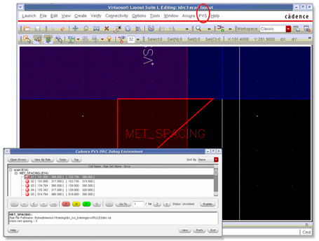
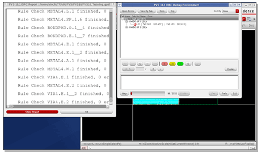
Time To Error
Error Browser will pop up and allow viewing of errors while job is still running.
PVS LVS
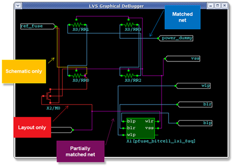
Rapidly identifies complex LVS mismatches
|
Graphic LVS Debug accelerates identification of complex LVS mismatches in chip designs |
|---|---|
- Compares logical and physical design using a common schematic representation |
|
- Guides navigation using design errors |
|
- Can be launched with LVS debug environment, and graphical elements can be probed through the LVS debug environment |
|
- All errors and warnings are easily navigated and show surrounding context |
Strong functionalities and flexible usability
|
Error Tags |
|---|---|
|
World view or detail view |
|
Filter net, devices for better understanding of error |
|
Drill down for more information on points of interest |
|
etc |
LVS Hyper debugger - Graphical LVS Debug
LVS debug is extremely time-consuming and experience dependent
|
Limitation of current tools |
|---|---|
- Static error report in batch mode, contain large data, difficult to understand |
|
- Errors in text report hard to identify relationship |
|
- User cannot actively query more information on points of interest |
|
- Not allow easy navigation of the original design |
|
|
Bind-key - Cadence Composor like |
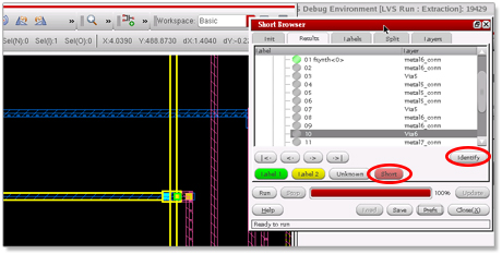
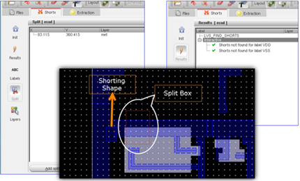
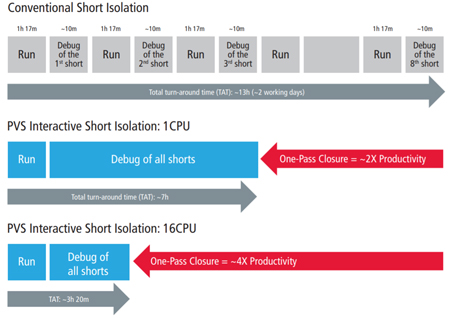
One-pass short isolation
|
Locating shorts found in old-fashion LVS comparison report requires |
|---|---|
- Additional manual work |
|
- Additional LVS extraction and comparison runs |
|
|
PVS approach facilitates one-pass short isolation for cell / block / full-chip designs |
- Run time typically <10% of extraction time and scales up to 5x with 8 CPUs |
|
- Start debugging while run is in progress as soon as first results are available |
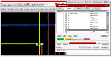
Interactive Short Locator - Comparison with and without the Interactive Short Locator
PVS to QRC interface
Fully solution for back-end verification
Support Cadence QRC flow to complete post-layout simulation
|
No additional licenses required to enable flow |
|---|---|
|
Provides complete QRC GUI support |
|
TECHLIB feature makes PVS QRC flow easy to use |
|
Batch / interactive use model |
|
Support Spice, SPEF, DSPF, extracted view, etc. flows |
|
Parity of flow between PVS / Assura = easy transition |